Engineers use FPGAs to test different hardware designs and explore new devices. They’re also practical for building/prototyping embedded and industrial applications. Boards from Lattice, Terasic, and AMD offer varying capabilities, such as secure boot control and high-speed processing. These also handle sensor interfacing and I/O expansion. The following are the lowest power, and newest, FPGAs.
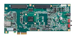 The Lattice Mach-N2 Evaluation Board.
In September 2026, Lattice introduced its Mach-N2 (LN2-MH-20-EVN) Evaluation Board for prototyping and evaluating low-power, secure control FPGA applications. It has 220,000 system logic cells, LPDDR4 memory, integrated flash, and hardware security.
For connectivity, the board comes with 4x PCIe Gen4, 2x FMC expansion connectors (HPC, LPC), a Raspberry Pi MIPI Camera connector, and 1G Ethernet. Switches, pushbuttons, user LEDs, and configuration jumpers are also included. Developers can use the board to develop secure network infrastructure, always-on system control, and high-speed data interfaces.
The Mach-N2 features PUF-based security, user run-time security, and CNSA 2.0-compliant, post-quantum cryptography with crypto agility on the root-of-trust device. In addition, the integrated non-volatile flash protects FPGA configuration and enables single-chip boot in < 30 ms.
- GPIO breakout with two FMC connectors (FMC-1 and FMC-2), Raspberry Pi MIPI Camera connectors, and Ethernet
- Uses 220,000 system logic cells
- 12-Mb embedded memory
- 94 wide-range I/O pins and 153 high-speed differential I/O pins
- Mini USB-B connection for device programming
- 8x DIP switches, 3x pushbuttons, 8x green LEDs, and 3x seven-segment LEDs (designed configuration)
- PCIe Gen4 x4 finger edge
- Reference clock sources
- Lattice Radiant software programming support
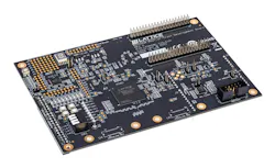 Lattice’s MachXO4 RoT Development Board handles applications such as secure boot and hardware management.
The Lattice MachXO4 RoT Development Board is for engineers who want to explore the MachXO4 RoT FPGA. This allows them to rapidly prototype and test hardware management and security applications. It features an integrated cryptographic engine while supporting secure boot and hardware-based protection. Lattice’s MachXO4 RoT also has SPI flash (16 Mbit) for external storage.
Expansion options are included via Raspberry Pi, Arduino, Versa, FX12, and Aardvark headers. With these interfaces, developers can connect extra hardware and evaluate custom designs. Thanks to its low-power and integrated security, the board is practical for secure boot, hardware management, and low-power industrial control.
- Hardened Cryptographic Engine for secure boot and platform-security designs
- Up to 2,693-kb User Flash Memory (with dual-boot disabled)
- Instant-on operation (less than 5-ms boot time)
- GPIO interface for connecting to Arduino and Raspberry Pi boards
- USB-B port for device programming and Inter-Integrated Circuit (I2C) communication
- 16-Mb Serial Peripheral Interface (SPI) flash with quad-read support
- Up to 381 I/O pins (484-ball caBGA package)
- 4-position DIP switches, 4 pushbuttons, and 16 LEDs for demonstration Lattice Radiant programming support
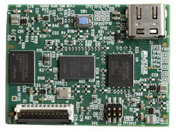 The Lattice CrossLinkU-NX SoM Development Kit.
Lattice unveiled its CrossLinkU-NX SoM Development Kit for prototyping low-power edge AI and embedded system applications. Running on the CrossLinkU-NX FPGA, this system-on-module has an always-on feature for power efficiency. It also has MIPI CSI-2 camera input, USB 3.1 device interface, and digital I/O.
Users can pair the kit with a carrier card to connect a Raspberry Pi CM5 with the CrossLinkU-NX SoM. This provides extra connectivity via 1G Ethernet, microSD storage, GPIO interface, and USB 3.1 host. Both modules also come with debug connections. The development kit can be used for camera interfaces, edge AI, and embedded vision.
- Four-lane MIPI CSI-2 receiver with Soft D-PHY
- Supports low-power always-on operation
- 64-Mb HyperRAM memory
- 512-Mb SPI flash
- 22-pin Raspberry Pi camera connector
- USB Type-C connectivity (USB aggregation)
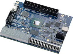 Terasic’s DE23-Lite Development Kit is powered by the Altera Agilex 3.
Priced at $169, the Terasic DE23-Lite Development Kit is an FPGA platform running on an Altera Agilex 3 with 135,110 logic elements. The board also has SDRAM (64 MB), an integrated ADC, GPIO expansion interfaces, and HDMI output. Developers can use the USB-C connectivity for FPGA programming. Other resources are for testing and prototyping, such as LEDs, onboard switches, and seven-segment displays.
The DE23-Lite development kit is suitable for robotics, digital logic prototyping, video processing, FPGA edge applications, and power-efficient embedded vision.
- Altera Agilex 3 A3CZ135BB18AE75 FPGA (135,110 logic elements)
- 89-Mb M20K and 1.4-Mb MLAB embedded memory
- 368 18x19 hardware multipliers
- SDRAM (64 MB)
- 128-Mb QSPI configuration flash
- HDMI output with audio
- USB Type-C with USB Blaster III programming support
- GPIO and ADC expansion headers
- 10 LEDs, 10 slide switches, 4 pushbuttons, and 6 seven-segment displays
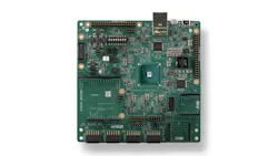 The AMD Spartan UltraScale+ SCU35 Evaluation Kit.
AMD’s Spartan UltraScale+ SCU35 Evaluation Kit ($229) is a platform for developing FPGA-based sensor interfaces and board-management systems. It runs on the AMD Spartan UltraScale+ SU35P FPGA, which has 36,000 logic cells. It supports various peripheral connections and features four Pmod connectors, two MikroE Click ports, an Arduino Shield interface, and two Raspberry Pi HAT expansion interfaces. With this setup, developers can connect and experiment with sensors and hardware modules.
In addition, 64-Mbit HyperRAM, Ethernet connectivity, and power-monitoring devices are included. These track how much power is consumed by a system. Thanks to support from AMD Vivado and Vitis development tools, this kit is well-suited for prototyping I/O expansion and management operations for medical, industrial, and data center equipment.
- Spartan UltraScale+ SU35P FPGA (36,000 logic cells)
- Up to 304 total I/O
- On-chip memory (1.93 Mb)
- 64-Mb HyperRAM
- 4x Pmod connectors, 2x MikroE Click ports
- 1x SYZGY high-speed I/O connector
- Arduino Shield and 2x Raspberry Pi HAT expansion interfaces
- 10/100 Ethernet with RJ-45 connector
- Hardware security features
Source: Electronic Design